Three facts set the frame, and none of them fits the usual story about memory.
DDR6 has no published standard. JEDEC still lists it as a project in the JC-42 committee, alongside HBM5, while the current desktop and server document remains DDR5 [2].
LPDDR6 does have a published standard, and it shipped: in September 2026, CXMT announced mass production at 12.8 Gbps, debuting in Xiaomi’s 18 Fold [3].
And CXMT, which put its first 8Gb DDR4 into volume production in 2019, held 9.5% of global DRAM revenue in the second quarter of 2026 [3]. The company whose rise prompted this post [1] is now the fourth supplier in a market that had three for two decades.
So the question “DDR3, DDR4, DDR5, DDR6, DDR7?” has a short answer and a long one. The short answer: DDR7 does not exist, DDR6 is a draft, and the interesting movement is in the low-power branch. The long answer is the ladder itself.
Two ladders, not one
DDR and LPDDR are separate standards with separate documents, and the numbers do not correspond. LPDDR5 is not “DDR5 for phones”; it is a different interface that happened to be standardised in the same era [5].
The difference is physical. DDR is built around modules: a 64-bit data path per DIMM, a socket, a serial presence detect chip, and since DDR5 a power management chip on the module itself [6]. LPDDR is built around packages soldered to a board: narrower channels, fewer pins, lower voltages, and a command bus designed to keep a phone’s power budget intact.
That is why the two ladders diverge. A DDR5 DIMM splits its 64 pins into two 32-bit subchannels, each with its own command bus, and doubles the minimum burst to 16 transfers so a cache line still arrives in one access [6]. LPDDR5 keeps two 16-bit channels per die. LPDDR6 narrows further, to two 12-bit subchannels with four command and address lines each and an access granularity of 32 bytes [7].
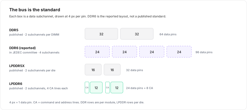
The subchannel split is the standard’s real identity, more than its data rate
The ladder, as documented
| Standard | Document | Published | Rate (MT/s) | Data channel | GB/s per 64 data pins at top rate | What changed |
|---|---|---|---|---|---|---|
| DDR3 | JESD79-3F | 2007, rev. 2012 [8] | 800 to 2,133 | 64-bit | 17.1 | 8n prefetch, fly-by topology, 1.5 V, 1.35 V low-voltage variant |
| DDR4 | JESD79-4D | 2012, rev. 2021 [9] | 1,600 to 3,200 | 64-bit | 25.6 | bank groups, 1.2 V, higher density per die |
| DDR5 | JESD79-5D | 2020, rev. 2025 [2] | 4,800 to 6,400 | 2 x 32-bit | 51.2 | two subchannels per DIMM, burst 16, on-die ECC, PMIC on module [6] |
| DDR6 | not published | in committee [2] | 8,800 to 17,600 reported [10] | 4 x 24-bit reported [11] | 140.8 | decision feedback equalisation, CAMM2 modules reported [11] |
| LPDDR4X | JESD209-4-1 | 2017 [5] | up to 4,266 | 2 x 16-bit | 34.1 | I/O voltage cut to 0.6 V [5] |
| LPDDR5 | JESD209-5 | 2019 [5] | up to 6,400 | 2 x 16-bit | 51.2 | WCK clock, write-X, 16-bit channels [5] |
| LPDDR5X | JESD209-5B | 2021 [5] | 8,533, later 9,600 | 2 x 16-bit | 76.8 | faster I/O on the same array; Samsung parts reach 10.7 Gbps [5] |
| LPDDR6 | JESD209-6 | 2025 [2] | 10,667 to 14,400 reported | 2 x 12-bit | 115.2 | 32-byte granularity, DVFSL, per-row activation counting, link ECC [7] |
Two readings of that table matter.
The first is that the generations are not evenly spaced in capability. DDR4 launched at twice DDR3’s opening rate and DDR5 at three times DDR4’s. DDR6 is projected to do it again, but the DDR5 standard is still moving underneath it: JEDEC’s MRDIMM work targets 12,800 MT/s on DDR5 hardware, with new buffer and clock-driver documents published in April 2026 [12]. A standard that keeps absorbing demand is a standard whose successor arrives late, and that is exactly what the roadmap now says: DDR6 commercialisation is expected in 2028 or 2029, not the 2027 that 2025 reporting predicted [10].
The second is that per-pin speed and total throughput are not the same claim. A 64-bit DDR5-6400 channel moves 51.2 GB/s. A 24-bit LPDDR6 channel at 14,400 moves 43.2 GB/s from 24 pins rather than 64. Per pin, LPDDR6 at 14,400 moves 2.25 times the data of DDR5-6400, which is why the low-power branch now runs faster per lane than any DDR5 part on sale, while staying far behind per module. On a phone, where pins and power are the constraint, that is the relevant number. On a server, where you can afford 64 pins and socketed modules, it is not.
DDR6 is a document-shaped hole
There is no JESD79-6. JEDEC’s own page says DDR6 and HBM5 are “in development”, which is the language it uses for work that members can see and the public cannot [2]. Everything else is reporting: a starting rate around 8,800 MT/s, a target of 17,600, four 24-bit subchannels in place of DDR5’s two 32-bit ones, decision feedback equalisation, and a possible move to CAMM2 modules because a DIMM socket struggles above 6,400 MT/s [10][11].
The 24-bit split is the interesting part. At 8,800 MT/s and above, a 32-bit subchannel sees enough crosstalk and reflection that equalisation alone stops being enough. Narrower slices lower the load per lane, at the cost of more command buses and a more complex module. It is the same trade LPDDR made years earlier, arriving in the desktop part of the ladder.
Meanwhile, the concrete work being funded is elsewhere. DRAM makers have asked substrate suppliers to start DDR6 prototypes, which is a real signal that the package, not the array, is the long pole [10]. And the money being spent on memory in 2026 is going into HBM, which is why JEDEC’s other active project is HBM5 [2].
DDR7 does not exist. GDDR7 does.
This is the confusion worth clearing up early.
There is no DDR7 standard, no JEDEC project for one, and no published roadmap in which it appears. The next desktop generation after DDR6 is not yet named, because DDR6 is not yet finished.
GDDR7, on the other hand, exists: JESD239, published in March 2024, the first JEDEC DRAM standard to use PAM3 signalling, with four independent channels per device and up to 192 GB/s per chip [13]. It is a graphics bus, optimised for a GPU’s short, wide traces and enormous bandwidth per pin, and it has nothing to do with the DIMM in a desktop.
Where the name comes from is not mysterious. A GPU spec sheet says “GDDR7”. A phone says “LPDDR6”. A desktop says “DDR5”. The three ladders are adjacent, use overlapping vocabulary, and are not interchangeable. LPDDR6 is the sixth low-power generation, not the mobile edition of DDR6.
What comes after DDR6 will most likely be an extension of the same pattern: DDR6 revisions, LPDDR6 variants aimed at data centres, HBM4 and HBM5, and eventually 3D DRAM. The last of those is no longer only a roadmap line: an 8-layer stacked oxide-semiconductor DRAM cell transistor was fabricated and reported at IEDM 2025 [24], a monolithic 3D design with BEOL oxide-channel access transistors followed at IMW 2025 [25], and Nature Electronics framed the approach as a route to high-density, low-power memory [23]. JEDEC has also previewed LPDDR6 work for server modules and processing-in-memory, a signal that the low-power ladder is no longer only about phones [10].
What CXMT actually ships
The company is real, and so is the product list. The details below are what its own announcements and the trade press report, which is a different standard of evidence from a published JEDEC document.
| When | What |
|---|---|
| 2016 | Founded in Hefei with the municipal government, roughly RMB 18 billion for a 12-inch fab [4] |
| 2019 | 8Gb DDR4 in volume production, the first Chinese-designed DRAM to get there [4] |
| 2024 to 2025 | DDR5 on a 17nm-class process; DDR5 dies reach 90% yield, and GIGABYTE validates CXMT dies across its DDR5 boards up to 8,200 MT/s [16] |
| 2025 | IEDM papers on a monolithically integrated 3D FeRAM and a BEOL-integrated multi-layer DRAM, both described as firsts [21] |
| Sept 2026 | G5 platform in mass production: 11.95nm active-area half-pitch with SAQP, 45:1 capacitor aspect ratio, HKMG, at least 50% more dies per wafer; 24Gb LPDDR5X in 496-ball and 245-ball packages [14][15] |
| Sept 2026 | LPDDR6 mass production at 12.8 Gbps peak, 10,667 with the SoC, 16GB package from 16Gb dies in a 1,295-ball FBGA, debuting in the Xiaomi 18 Fold [3] |
| End 2026 | Server DDR5 RDIMMs built on a 4F² cell architecture, with a vertical surrounded gate [17] |
| 2026 | HBM3 samples to Alibaba T-Head and Cambricon; HBM3E limited production planned within two months [19][20] |
The DDR5 numbers are the ones that unsettled the incumbents. A 48GB kit on a Colorful X870E board reached 4,507 MHz, or 9,014 MT/s effective, in August 2026, up from the 8,000 MT/s CXMT claimed in late 2025 [16]. That is overclocking, not a JEDEC grade, and it came with CL30 timings and a CL28 target. Ten years ago a new entrant shipping DDR5 at 90% yield on DUV-only lithography would have been the story of the decade; in 2026 it is a line item before the LPDDR6 paragraph.
Two claims in that table need separating. G5 is a process announcement, and the useful parts are geometric: an 11.95nm half-pitch, a 45:1 capacitor, and 50% more dies per wafer than G4 [15]. The 24Gb LPDDR5X parts are products, in mass production, in two package sizes [14]. The first is evidence of manufacturing capability. The second is evidence of commercial intent.
One number in the source profile is easy to misread. It credits Zhu Yiming personally with 169 patent applications and 104 granted patents [1]. That is an inventor’s record, not the company’s portfolio: a 2024 ranking of mainland semiconductor manufacturers put CXMT at 13,449 patents, second overall [21]. Both numbers are real, and they measure different things.
How, without EUV
China’s fabs work without EUV, and export controls keep the most advanced lithography out [1]. CXMT’s answer is brute-force patterning: self-aligned quadruple patterning to push a DUV scanner past what a single exposure can resolve, plus a digital twin of the process to tune it without burning wafers [15].
SAQP is not a shortcut. Each additional spacer step multiplies sensitivity to mandrel width, deposition uniformity, and etch variation, and the accumulated error shows up as pitch walk: uneven spacing that turns into timing and yield problems downstream [15]. Getting it into volume production is the achievement. The metrology literature treats pitch walk and critical-dimension uniformity as the defining control problem of the process, because errors accumulate through every deposition and etch step [31], and it explains why the process node race reads differently for CXMT. The company is not at 1-beta or 1-gamma. It is at a 17nm-class node with aggressive multipatterning, and it is closing the density gap with geometry rather than with a smaller transistor.
The 4F² announcement is the next step in that logic: four features squared instead of six, a vertical gate for electrostatic control, and hybrid bonding to separate the cell array from the peripheral CMOS [17]. CXMT says it holds more than 300 published patent families on the approach and will ship a DDR5 RDIMM using it before the end of 2026 [17]. Samsung showed a 4F² prototype at ISSCC 2026 and is not expected to commercialise before 2028 [17]. A year-end product would put CXMT ahead of Samsung on a technology Samsung has been researching longer, which is the kind of claim that deserves a shipment date before it deserves belief. The architecture class is not speculative: SK hynix’s VLSI 2026 4F2 vertical-gate demonstration puts the periphery under the cell array by wafer bonding and adds a shared back gate between word-line pillars [29].
The other bet: 3D FeRAM
DRAM stores a charge that leaks, which is why it refreshes every 32 ms up to 85 C [6]. FeRAM stores a polarization state that does not leak, in a ferroelectric capacitor, which makes it non-volatile, fast, and low-voltage: with HfO2 films the write voltage can sit below 1 V, endurance goes beyond 1e12 cycles, and retention past ten years for a 1T1C cell with clean interfaces [22].
The catch is the physics that has kept FeRAM in niche markets. Read margin is proportional to capacitor area, so shrinking the cell shrinks the signal [22]. The field’s answer looks like 3D NAND: build the capacitor vertically and stack layers, either as a NAND-like parallel stack or as sequential BEOL layers on top of logic [22]. CEA-Leti demonstrated the BEOL version at 22nm in June 2026: a 0.047 µm² 1T1C bitcell operating at 1.3 V with a 4:1 vertical HZO capacitor, and a path to a 17:1 aspect ratio at 0.0028 µm² [26]. HfO2’s ferroelectricity, first reported in 2011, is what made the material compatible enough with CMOS processing to try [30]. The phase is metastable, though: doping, anneal and substrate set the microstructure, and the resulting defect population is what sets device reliability, which is why the thesis literature on doped HfO2 reads as much about process control as about physics [32].
CXMT’s IEDM 2025 papers were two bets in that direction: a monolithically integrated stacked 3D FeRAM, and a BEOL-integrated multi-layer DRAM built with IGZO channel transistors, both presented as world firsts, in a year when CXMT had the most accepted papers of any Chinese company [21]. “Monolithic” is the operative word: the layers are built directly on top of the logic rather than bonded afterwards, which is the version that could sit above a CPU without a second die.
Read that as research, not product. Three things stand between a paper and a part: read margin and disturb management in a 3D array, where cells share word lines and plate lines; the thermal budget of BEOL processing, which has to leave the layers underneath intact; and the endurance of the cell type chosen. The 1T1C cell has good endurance and a destructive read; the FeFET has a nondestructive read and poor endurance, often below 1e6 cycles on silicon channels, with charge trapping identified as the dominant mechanism as soon as the first Si:HfO2 devices were integrated at 28nm [33]; the hybrid 2T-nC cell trades area and disturb complexity for a quasi-nondestructive read [22]. Each architecture is a different answer to which of those costs you can afford. IBM’s IEDM 2025 work pushes the hybrid cell toward hundreds of layers, demonstrating 2T-64C configurations and identifying a read-history dependence that needs a discharge scheme before the next read [27].
| Property | DRAM (DDR5) | FeRAM (1T1C) | 3D FeRAM |
|---|---|---|---|
| Stores | charge on a MIM capacitor [6] | remanent polarization in an MFM capacitor [22] | the same cell, stacked in layers [22] |
| Volatile | yes, refreshed every 32 ms up to 85 C [6] | no [22] | no [22] |
| Write voltage | 1.1 V I/O, higher internally | below 1 V across the ferroelectric film [22] | set by the stack |
| Read | nondestructive, sense amplifier | destructive in the charge-sensing cell, needs write-back [22] | set by the cell |
| Endurance | effectively unlimited while powered | above 1e12 cycles for the MFM capacitor [22] | set by cell and stack |
| Density lever | smaller node, taller capacitor, 4F² | capacitor area, so a vertical capacitor | number of layers [22] |
Why a DRAM maker cares: the capacitor aspect ratio is already 45:1 on G5 [15], and every generation makes that etch harder. A technology that stores state in polarization instead of charge removes the retention problem, and one that can be stacked removes the lithography problem. Neither solves the other’s density economics today. DRAM’s cost per bit is the output of decades of yield learning; FeRAM’s is not.
What to watch is not a FeRAM DIMM, and not DDR7. The plausible near-term use is embedded memory and edge devices, where non-volatility and low write energy are worth more than the last factor of density. The 3D versions are a bet that layer count becomes the density lever, the way it did for NAND.
The part that is not going well
HBM is the wall.
CXMT’s HBM3 8-high parts are reported at roughly 30% front-end yield, with about 70% of survivors passing back-end test, which lands near 25% final yield against a 90% benchmark at SK hynix [19]. The cause is not the DRAM process, which is described as fine on the G4 node, but through-silicon vias and stacking: CXMT is reported at around 3,000 TSVs per die against more than 8,000 for SK hynix’s HBM3, and fewer vias is a way to lower difficulty at the cost of bandwidth [19]. The company is sampling to Chinese AI chip designers and planning limited HBM3E output at 20% to 30% yields [20]. Stacking yield multiplies in a way that explains why this is hard to buy your way out of: an 8-high hybrid-bonded die stack measured 94% to 95% per-layer yield, which lands at 58% void-free and 68% electrical for the complete stack [28].
That is the honest shape of the challenge. Commodity DRAM rewards a good enough cell and a cheap wafer. HBM rewards a decade of packaging know-how, and packaging is where the incumbents’ advantage compounds.
Reading the ladder correctly
Four rules make the reporting easier to read.
Published is not announced. JESD79-5D is a document [2]. “DDR6 at 17,600” is a target in a trade-press report [10]. “LPDDR6 at 12.8 Gbps” is a product announcement with a device in a phone [3]. Each is evidence of something different.
A generation is a bus, not a speed. LPDDR6 at 14,400 beats DDR5 at 6,400 per pin and loses per channel, because 24 pins are not 64. The comparison only means something once you fix the width and the workload.
The successor arrives when the incumbent stops absorbing demand. DDR5 has MRDIMM at 12,800 in the works [12], and DDR6 slipped to 2028 or 2029 [10]. Standards do not replace standards; economics does.
One boundary is worth stating. Three load-bearing facts here are reporting rather than documents: DDR6’s four 24-bit subchannels, the year-end 4F² RDIMM target, and the HBM yield figures. Each would be settled by a different artifact, a published JESD79-6, a shipping part that can be examined, or an audited yield disclosure, and each is labelled where it appears. The rest of the ladder rests on public standards and peer-reviewed results.
The entrant wins at the bottom first. CXMT’s share went from 7.6% to 9.5% in one quarter by selling DDR5 and LPDDR5 into a shortage, at prices 5% to 10% below Samsung and SK hynix, with capacity booked through 2027 [16][3]. That is the commodity ladder working as designed. HBM is a different ladder, and the company is at the bottom of it.
The IPO is the clearest expression of the same asymmetry. Priced at RMB 8.66, it traded as high as 49.50, rose 471.6% on the first day, and left CXMT with a market capitalisation of about RMB 3.3 trillion, briefly above Intel’s [18]. The company raised RMB 57.9 billion and expects first-half 2026 net profit of RMB 50 to 57 billion, against a loss of RMB 2.3 billion a year earlier [18]. Those numbers describe a supplier that arrived precisely when memory became scarce, not a supplier that out-engineered the incumbents.
Which is the useful conclusion. The ladder is a set of documents, a set of factories, and a set of prices, and CXMT’s rise is mostly the second and third. DDR6 will arrive when DDR5 stops being the cheaper answer. DDR7 will get a name when DDR6 stops being the newer one. And LPDDR6, the one part of the ladder that already shipped, is the reminder that the mobile branch has been the faster-moving one for a decade.
References
[1] Doanh nhân đứng sau CXMT: Kỹ sư từ bỏ lương để viết lại cuộc chơi chip nhớ toàn cầu: the profile of Zhu Yiming and CXMT that prompted this post, including the claim that export controls limit access to advanced lithography.
[2] JEDEC, Main Memory: DDR SDRAM, HBM: states that DDR6 and HBM5 are in development, that JESD79-5D is the current DDR5 revision (November 2025), and that LPDDR6 was published as JESD209-6 in July 2025.
[3] TrendForce, CXMT Starts LPDDR6 Mass Production at 12,800Mbps: the 12.8 Gbps peak, the 10,667 Mbps SoC rate, the 16GB package from 16Gb dies, the Xiaomi 18 Fold debut, the company’s 60% bandwidth and 20% power claims, and the 9.5% second-quarter revenue share.
[4] TrendForce, How Founder Zhu Yiming Built China’s DRAM Challenger: the 2016 founding, the RMB 18 billion fab investment, the 2019 8Gb DDR4 volume production, and the accumulated losses through 2025.
[5] Wikipedia, LPDDR: generation dates and rate grades for LPDDR4X (published March 2017, 4,266 MT/s, 0.6 V I/O), LPDDR5 (February 2019), and LPDDR5X (July 2021, later extended to 9,600 MT/s), and the point that LPDDR and DDR numbering do not correspond.
[6] Wikipedia, DDR5 SDRAM: the two 32-bit subchannels per DIMM, the doubled burst length of 16, on-die ECC, the 1.1 V supply, and the on-module PMIC.
[7] JEDEC, LPDDR6 Standard press release: two 12-bit subchannels with four command/address lines each, 32-byte access granularity, DVFSL, per-row activation counting, and link protection.
[8] JEDEC, DDR3 SDRAM Standard JESD79-3F: the current DDR3 document, published July 2012.
[9] JEDEC, DDR4 SDRAM Standard JESD79-4D: the current DDR4 document, published July 2021.
[10] IntuitionLabs, DDR6 Explained: the October 2026 status check, the 2028 to 2029 commercialisation shift, the reported 8,800 to 17,600 MT/s range, the four 24-bit subchannel proposal, and JEDEC’s LPDDR6 data-centre and PIM preview.
[11] Wikipedia, DDR6 SDRAM: the reported 8,700 to 17,600 MT/s range, four 24-bit channels, CAMM2 modules, and decision feedback equalisation.
[12] JEDEC, DDR5 MRDIMM ecosystem announcement: the April 2026 data-buffer and clock-driver documents, and the Gen2 raw card designs targeting 12,800 MT/s.
[13] JEDEC, GDDR7 press release: JESD239, March 2024, PAM3 signalling, four independent channels, and up to 192 GB/s per device.
[14] CXMT, G5 platform announcement: the 11.95nm active-area half-pitch, 45:1 aspect ratio, 6,762nm cell array height, 50% dies-per-wafer gain, and the two 24Gb LPDDR5X packages.
[15] TrendForce, CXMT G5 DRAM Enters Mass Production: the SAQP description, the pitch-walk risk, the DUV limits at 1-beta, and the relation between G5 and the LPDDR5X products.
[16] TrendForce, CXMT DDR5 Tops 9,000 MT/s: the 9,014 MT/s overclock, the 90% yield on 17nm-class DDR5, GIGABYTE validation to 8,200 MT/s, the 7.6% first-quarter share, the capacity path from 300,000 to 350,000 wafers per month, and the 5% to 10% price discount.
[17] TrendForce, CXMT Accelerates 4F² DRAM Push: the vertical surrounded gate, the 300-plus patent families, the year-end RDIMM target, Samsung’s 2028 timeline, and the 9.5% second-quarter share against Samsung, SK hynix and Micron.
[18] TrendForce, CXMT’s 471% STAR Debut: the RMB 8.66 offer price, the 49.50 intraday high, the 471.6% first-day gain, the RMB 3.3 trillion market capitalisation, the RMB 57.9 billion raised, the first-half profit guidance, and the ByteDance supply agreement.
[19] ChosunBiz, CXMT lags in HBM3 yields: the roughly 30% front-end and 25% final HBM3 yield, the 3,000 versus 8,000 TSV comparison, and the samples to Alibaba T-Head and Cambricon.
[20] Reuters, China’s CXMT to start advanced AI memory production despite poor yields: the 20% to 30% HBM3E yields and the plan for limited production within two months.
[21] Sina, CXMT’s two IEDM breakthroughs: the monolithically integrated 3D FeRAM and the BEOL-integrated multi-layer DRAM with IGZO channels, the claim that both are firsts and that CXMT had the most accepted IEDM papers among Chinese companies, and the 13,449-patent ranking.
[22] A Full Spectrum of 3D Ferroelectric Memory Architectures Shaped by Polarization Sensing: the 1T1C cell’s sub-1V HfO2 write, above 1e12-cycle endurance and ten-year retention, the sense margin that scales with capacitor area, the 1T1C, FeFET and 2T-nC trade-offs, and the parallel versus BEOL stacking options.
[23] Song and Khan, 3D DRAM with stacked oxide-semiconductor channel transistors, Nature Electronics 8, 1132-1133 (2025): the case for oxide-semiconductor channel transistors in a 3D DRAM, and the IEDM 2025 result it discusses.
[24] Okajima et al., Highly stackable oxide-semiconductor channel transistor technology for future high-density and low-power 3D DRAM, IEDM 2025: an 8-layer stacked OCTRAM cell transistor, fabricated and measured across all layers.
[25] Monolithic 3D Stackable DRAM Design with BEOL-Compatible Oxide Channel Access Transistor, IEEE International Memory Workshop 2025: the monolithic variant, with the access transistor built above the array in the back end.
[26] CEA-Leti, Engineering 3D HZO Ferroelectric Capacitors to Scale Down 22nm Embedded FeRAM, VLSI 2026: the 0.047 µm² bitcell at 1.3 V, the 4:1 aspect ratio, the 17:1 and 0.0028 µm² path, and the wake-up-free behaviour.
[27] Duan et al., Towards Scalable 3D Integration of 2T-nC FeRAM with Hundreds of Layer Stacking, IEDM 2025: 2T-64C cells, the floating-node parasitic capacitance, the read-history dependence, and the FN discharge trade-off.
[28] Workman et al., Reliability and Yield for Die-to-Wafer Hybrid Bonded 8-High Stacks with TSV, IEEE Hybrid Bonding Symposium 2026: 94% to 95% per-layer yield, 58% void-free and 68% electrical full-stack yield, and the particle-driven void mechanism.
[29] Park, Electrical Characteristics of the 4F2 Vertical Gate DRAM with Bit-Line Shielding and Back Gate, SK hynix Research, VLSI 2026: the peri-under-cell wafer-bonding scheme, the shared back gate between word-line pillars, and the bit-line shielding.
[30] Böscke et al., Ferroelectricity in hafnium oxide thin films, Applied Physics Letters 99, 102903 (2011): the first report of ferroelectricity in HfO2, the material that made CMOS-compatible FeRAM possible.
[31] Chao et al., Advanced in-line metrology strategy for self-aligned quadruple patterning, SPIE Advanced Lithography 2016: pitch walk and critical-dimension non-uniformity as accumulated error across SAQP’s deposition and etch steps.
[32] Lederer, Material development of doped hafnium oxide for non-volatile ferroelectric memory application, doctoral thesis, TU Dresden (2022): the metastable ferroelectric phase, the dependence of microstructure on doping, substrate and anneal, and the resulting reliability behaviour.
[33] Yurchuk, Electrical Characterisation of Ferroelectric Field Effect Transistors based on Ferroelectric HfO2 Thin Films, doctoral thesis, TU Dresden (2015): the first Si:HfO2 FeFETs integrated in high-k metal gate CMOS down to 28nm, and charge trapping as the phenomenon that dominates their behaviour.